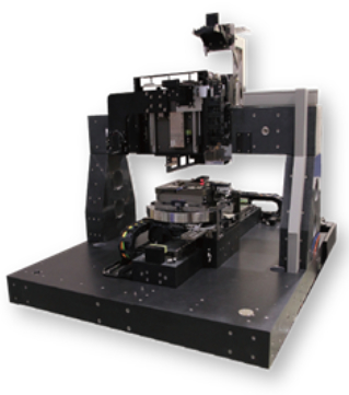
Industry Applications
Automated Optical Inspection
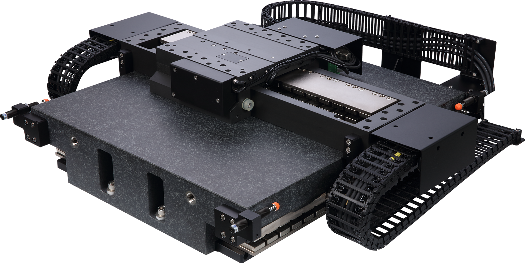
Inspection of nanometer-scale features requires absolute stability and zero-vibration motion to ensure image clarity and defect detection accuracy.
TOYO Linear Motor stages provide direct-drive precision with no mechanical backlash or vibration, while air bearings, active or passive vibration dampers, and large granite solutions eliminate additional vibration concerns and ensure thermal stability.
- High Scanning Speed: Rapid transit between inspection points without settling time delays.
- Sub-micron Repeatability: Ensuring consistent inspection results across millions of cycles.
- Air Bearing Compatibility: Optional integration for the most demanding frictionless environments.
- Environmental Stability: Vibration suppressing tools and system thermal management ensure maximum throughput for your system.
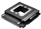
Wafer Handling
TOYO understands moving the wafer between workstations or loading and unloading the FOUP must be done without particle contamination or mechanical stress.
Sealed cleanroom actuators with vacuum suction ports eliminate particle emission.
- ISO Class 4 Compliance: Specialized seals and lubricants for fab-ready performance.
- Gentle Acceleration: S-curve motion profiling to prevent wafer slippage.
- Compact Footprint: High power density to fit within standard EFEM modules.

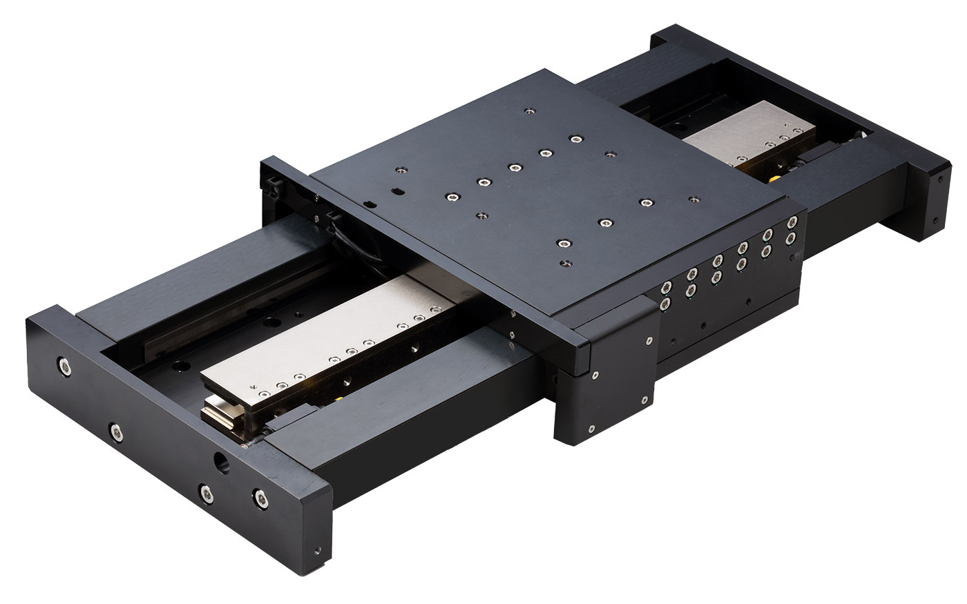
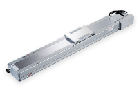
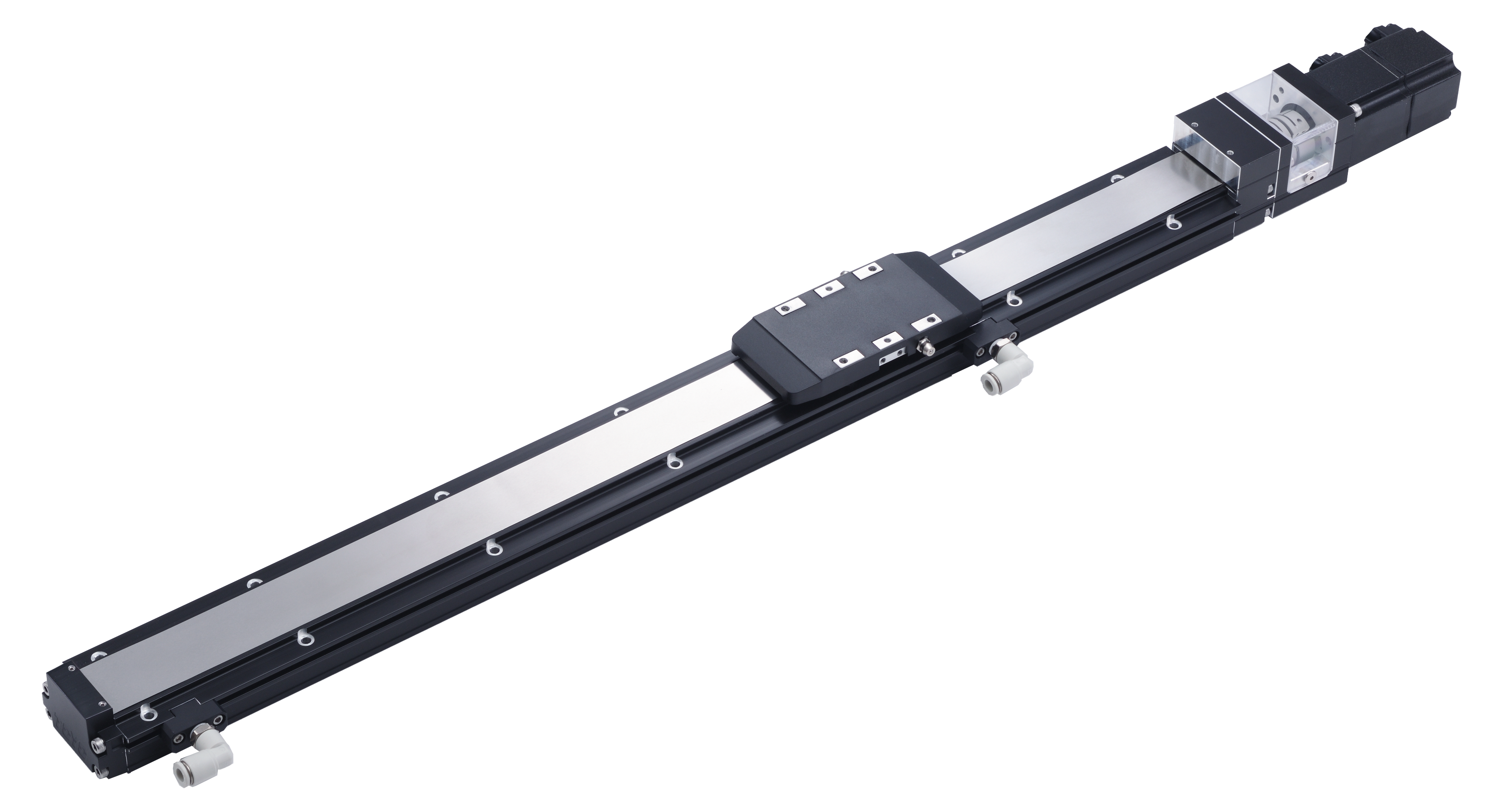
FOUP Transport
Managing FOUP (Front Opening Unified Pod) movement requires robust, high-speed motion that maintains cleanroom integrity over long strokes.
Belt-driven actuators optimized for high-speed, long-distance transport with low particle generation.
- Long Travel Capability: Systems engineered for overhead transport or fab-wide distribution.
- High Reliability: Low-maintenance belt designs for continuous 24/7 operation.
- Vibration Damping: Specialized mounting and drive logic to protect FOUP contents.
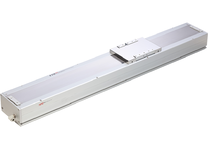
Wafer Dicing
Whether you are dicing via blade, laser, or plasma - TOYO understands precision motion is critical to the process.
Precision crafted linear positioning systems fit to withstand the process while achieving high precision positioning
- Environmental Sealing: Protection against water spray and silicon dust.
- High Stiffness: Ball screw drives engineered for high-thrust processing loads.
- Thermal Stability: Materials selected to minimize expansion during high-duty cycles.
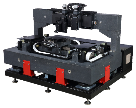
IC & Packaging
High-speed pick-and-place and bonding require extremely fast cycle times and precise force control for fragile interconnects.
Integrated motor-drive systems for ultra-fast response and high-speed multi-axis coordination.
- High Acceleration: Up to 3G acceleration for industry-leading cycle times.
- Force Feedback: Integrated sensing for delicate part placement.
- Multi-Axis Synchronization: Seamless control for complex wire-bonding or flip-chip processes.